Update: NXP finally released an app note detailing what each part is for: AN11392 - Guidelines for full-speed USB on NXP's LPC microcontrollers (19 Feb 2014). Some of what I guessed below is right, while some is misleading, and it appears that the Sparkfun circuit doesn't even follow the specification. Notes above in my 2 Apr 2014 entry.
I am trying very hard to use all of my components within their specifications. One part that was having trouble was the power switch in the power supply.
First, a look at the power supply:
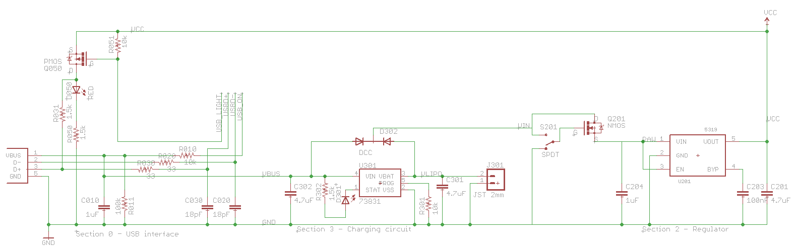
Let's take a closer look at the USB part:

For Google, this is the USB to LPC2148 SOFTCONNECT INTERFACE
Parts list:
| Quantity | Digikey Part | Value | Device | Part Numbers |
|---|---|---|---|---|
| 2 | 490-1281-1-ND | 18pF | CAP0402-CAP | C020, C030 |
| 1 | 490-3890-1-ND | 1μF | CAP0402-CAP | C010 |
| 1 | 350-2029-1-ND | RED | LED0603 | D050 |
| 1 | 455-2562-1-ND | USB_MICROB_JST | USB_MICROB_JST | J001 |
| 1 | BSS84-FDICT-ND | PMOS | MOSFET-PCHANNELSMD | Q050 |
| 2 | P10.0KLCT-ND | 10k | RESISTOR0402-RES | R010, R051 |
| 1 | P100KLCT-ND | 100k | RESISTOR0402-RES | R011 |
| 2 | P33.0LCT-ND | 33 | RESISTOR0402-RES | R020, R030 |
| 2 | P1.50KLCT-ND | 1.5k | RESISTOR0402-RES | R031, R050 |
A bit about the genealogy of this circuit. I originally got it from the Sparkfun Logomatic, which apparently was adapted from the Keil MCB2140 board, as explained by microbuilder.eu. All of these parts have a bunch of stuff not explained anywhere, and not mentioned on the LPC2148 datasheet, as seen below:

I have made some further adaptations to reduce the pin count and eliminate the vile BJT transistor in favor of a good and virtuous FET. Someday I will explain why FETs are better, but they are. Use FETs when you can, and BJTs when you have to.
So, in part number order:
- C010 is required by the USB spec. There must be between 1μF and 10μF between Vbus and Gnd as seen from upstream. If there is too little, the downstream device could be damaged by inductive flyback from the wire as it is disconnected. If there is too much, the inrush current to charge all that capacitance will be too high. The Sparkfun circuit had 0.1μF here, seemingly out of spec, but as it turns out, some of the capacitors downstream in the charger circuit are visible also. The Sparkfun circuit as a whole is within specs. This capacitor used to be higher until I noticed all the capacitance visible downstream.
- R010 and R011 seem to be there to provide pull-up and pull-down if the USB plug is unplugged or shorted. If the plug is unplugged, there is a total of 110kΩ of pull-down, so that the pin has a defined non-floating value if it is input. If Vbus and Gnd are shorted, there is still 10kΩ of pull-down, and more importantly, if the controller pin is output and high, there is 10kΩ of current limit.
- R020 and R030 are required by the USB spec. There must be between 28Ω and 44Ω of termination resistance. Accounting for the internals of the LPC2148, there must be a 33Ω resistor in series with each data line, as called out by the data sheet above.
- C020 and C030, form the other half of a low-pass noise filter, when combined with R020 and R030. In this case, frequencies higher than 250MHz are filtered out. This prevents the channel from being used as a high-speed (480MHz) channel, but the LPC2148 isn't capable of this anyway.
- R031 is required by the USB spec. When the downstream device (in this case the LPC2148) is ready to communicate, it ties in a pull-up resistor to one of D- (if low-speed) or D+ (if full-speed). Since the LPC2148 is a full-speed device (12MHz, up to 12Mb/s) it ties to D+.
- Q050 is the SoftConnect switch. It is a P-channel FET used as a high-side switch, which takes a bit of explanation. In a P-channel device, the source is connected to high voltage, and the drain to ground. If the gate voltage is sufficiently lower than the source, the FET conducts. In this circuit, the source is connected to Vcc (3.3V) and the gate is connected to the USB_SOFTCONNECT (or USB_LIGHT) pin on the LPC2148. When that pin is low, the transistor turns on, and provides a low-resistance path to Vcc, in effect tying one end of R031 to Vcc, which tells the upstream host that this device is ready to communicate. When the pin is high, the transistor turns off, and that end of R031 is left floating.
- D050 and R050 form an LED chain which lights whenever Q050 is on, or in other words, when SoftConnect is activated.
- R051 is a pull-up resistor, so that when the LPC2148 is off or its SoftConnect pin is input (as it is just after reset) the transistor is off, since its gate is not floating.
On to the charging circuit. I use an MCP73831, programmed to charge at 100mA, since I am planning for a battery as small as 100mAh. I have added a diode network D302 since there is no clear description in the data sheet for the 73831 explaining what the circuit will do if there is USB power present but no battery. With this diode network, if USB is present but the battery is not, the USB line will directly power the load. If the battery is present but the USB is not, the battery will power the load. If both are present, the USB wins, and the charger just has to concern itself with the battery, not the load.
Finally, the regulator circuit, and why this entry is subtitled "You can't use an N-channel MOSFET as a high-side switch."
The regulator itself is a MIC5319, capable in principle of delivering 500mA. Not that this is needed with the IMUinator, but to provide for future design expansion. It is hooked up exactly as specified in its own datasheet. The interesting part is the switch between the regulator and battery. That switch is only rated for 100mA. So, I said, let's stick a FET in there. We pick a nice high-current, low resistance FET available in a SOT-23 package. Use the switch to turn on the FET, and the FET to turn on the resistor. And here is where I made my mistake. I chose an N-channel FET, because I wanted direct logic on the switch (switch on -> FET on) and I installed it on the high side so that the circuit would be grounded (except for a floating Vin) when the FET was off.
But, "You can't use an N-channel MOSFET as a high-side switch".The FET is more accurately a voltage-controlled resistor. When the gate-to-source voltage is high enough, the resistance drops, and effectively the FET is just a wire, with about 200mΩ of resistance. But, the voltage is gate-to-source, and the very fact of dropping resistance raises the source-to-ground voltage. The gate-to-ground voltage remains the same, but the gate-to-source voltage drops as the source-to-ground voltage rises. The switch turns itself off.
It's not quite this bad, but in a way it is worse. The device will find some stable in-between state, dependent on the voltage supplied and probably the load on the regulator output. This in-between state will not be high enough to actually do anything, but high enough to draw some power, and dissipate it right in the FET. With the USB plugged in, the input was about 4.67V and I was getting about 3.07V out of a 3.3V regulator, showing that the FET had stabilized at less than 3.3V, when I was expecting near 4.67V. When the battery was used, the value was about 2.7V, not even enough to run the LPC2148.
So, the possible solutions are:
- Use a P-channel FET. This is what I would do if I had caught the design flaw early enough. The circuit would be identical, just the opposite switch position would now be on. Unfortunately, P-channel FETs and N-channel FETs both have the same pin assignments, so the source on the P-channel is the same pin as the source on the N-channel. However, the P-channel FET needs to have its source connected to high voltage, not low, so the board design would have to change. Since I already waited almost three weeks for the board, I can't do this.
- Remove the FET entirely. This way we just connect the gate terminal on the board to the source, and use the mechanical switch as the main switch. Perfect if I could just remove that FET already soldered on the board, or if I built a new one with no FET, but I don't have those parts.
- Short the FET. Don't remove it, just put a wire over the FET from gate to source. This will guarantee the gate-to-source voltage is zero, and therefore that the FET is off all the time. In the mean time, the voltage applied to the gate is shorted past the source to the load.
Update the second 24 Apr 2013:
No comments:
Post a Comment