Lights 4 and 5 on the back of the second board (where I am installing the blue lights) won't light. As it happens, neither will any of 54-59, but we'll save that part of the story for later.
I remember the solder bridge between two pins, and one of those pins, A7, is involved with the lights that don't work. So, we carefully measure pin A7 and conclude that no matter how we program it, it acts like a high impedance. The natural conclusion is that it is burned out. So, run to Sparkfun, buy their last three ATmega328s, and a hot air rework station to pull the old chip. Carefully remove the old chip, taking care not to scorch the white paint on the board or blow away any of the passive components. When the chip comes off, it comes off great. Put in a new chip, verrrry carefully check continuity between each pin to make sure there are no bridges or missed joints. Fix a couple of missed joints. Guess what. The board acts exactly as it did.
So, that theory is shot. I might have burned out pins on this chip, but exactly the same pins? I think not. Now time to gather more evidence for another theory. Write up a program that listens for commands on the serial port and turns individual signals high or low, with the rest at high-Z. Signals 1 and 16 are both no good. What is going on?
The Arduino documentation says that you can use the analog input pins A0... as normal digital pins with the syntax pinMode(A0,OUTPUT); digitalWrite(A0,HI); etc. Which is in fact true, but only to a point. On an ATmega328, pins A6 and A7 are internally called ADC6 and ADC7, not PB...(ADC6) or anything like that. They are dedicated input pins. I had been planning (as in had a circut board made) to use A6 and A7 as Charlieplex lines 1 and 16. Guess which Charlieplex lines don't work... And guess which signals lights 4 and 5 (and 54-59) use...
I have no one to blame for this but myself. It was right on the Eagle schematic symbol the whole time that all the other A0... pins were secondary uses of GPIO pins, but A6 and A7 were only labeled as ADC. I guess the weird part is that the crystal inputs and reset line are alternate uses of GPIO lines, but A6 and A7 are not.
So, here's the plan. Lots of green wires, hot air, and razor blades, to hack D11 and D12 into P1 and P16. This will require giving up two multiplexers, which completely hashes my plan to use the GPS. At least this will let me test the charlieplex. Then, order 16 more blue lights, another FT232 and a correctly wired board which uses the crystal pins as two more digital outputs, allowing me to use D11 and D12 as multiplexer controllers on the next rev. NO getting a new board until all the green wires are fixed. Don't even touch Eagle until the last green wire is in place and CharlieTest works. Consider putting a LiPo battery power supply on the next board as well.
The moral of the story is keep working the problem until you find the problem, and don't guess. I have a nice new hot air rework station which works really well, and costs more than the LEDs combined. Oh well.
Tuesday, February 28, 2012

Friday, February 24, 2012
It's alive!
I finally invent something that works!
-- Dr Emmett Brown
Well, I have just built an honest to goodness Arduino, a round one connected to the most elaborate Charlieplex I have ever heard of... but no light on D13, so I can't even test it with the Hello World for microcontrollers, blinking a light. So, I used the ASCIITable example, to see if I can get code on the machine and have it run.
I made (at least) one mistake in the board design, and had to run what may be the shortest green wire ever. The FT232 datasheet clearly states that the TEST pin must be grounded, or the device will go into test mode and not show up on USB as expected. Well, I didn't ground TEST on the circuit board, and the device didn't work as expected. However, there is one bit of good news. The pin right next to it is ground. So, one bridge removed from the ATmega, and one added to the FT232, and we are ready to go.
First, load the ArduinoISP onto the Nano 3.0 I have.
Next, connect it to Project Precision, while the Nano is unplugged.
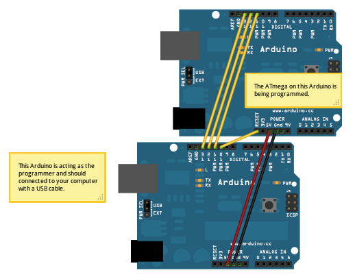 |
| Neither of the Arduinos involved look like this |
Next, plug everything in. First carefully check that the ribbon is plugged in right, then plug the Nano into USB.
Now run the bootloader instructions. All four lights on the Nano will light up simultaneously (something I hadn't seen before) and blink like crazy (except the blue power light).
 |
| Board the device and bring it to life! |
ASCII Table ~ Character Map
!, dec: 33, hex: 21, oct: 41, bin: 100001
", dec: 34, hex: 22, oct: 42, bin: 100010
#, dec: 35, hex: 23, oct: 43, bin: 100011
$, dec: 36, hex: 24, oct: 44, bin: 100100
%, dec: 37, hex: 25, oct: 45, bin: 100101
&, dec: 38, hex: 26, oct: 46, bin: 100110
', dec: 39, hex: 27, oct: 47, bin: 100111
(, dec: 40, hex: 28, oct: 50, bin: 101000
), dec: 41, hex: 29, oct: 51, bin: 101001
*, dec: 42, hex: 2A, oct: 52, bin: 101010
and so on for all 94 printable characters.
I wasn't happy with the stencil and solder paste on the edge of the board, So, on to soldering 240 surface mount LEDs by hand!
Thursday, February 23, 2012
Desktop Microscopy and Charlieplexing
One of the things I used to have to do with all my custom boards is take them into the lab at work. There they have a really nice optical microscope. This one looks at things instead of through things, so it is appropriate for electronics (funny that, being in an electronics lab). It doesn't have an eyepiece as much as it has a facepiece. The end you look through has a screen (pure optical, no electronics or cameras involved) about 5 inches wide. It gives you a stereo view with a single objective lens, because each of your eyes is looking through a different optical path in the same set of lenses.


I have been searching for something like that and finally restricted myself to something I could actually afford, a USB digital microscope. I ended up getting this microscope.
The subject of this particular set of pictures is Project Precision. For about five years now I have had a design in the back of my mind for a digital handed clock with an hour hand, minute hand, second hand and third hand (1 third = 1/60 second. Yes, really. Isaac Newton used thirds in the Principia.). I had a design using all 7400 series logic, a PIC and less 7400 logic, but finally came across the concept of charlieplexing. With 16 pins, I can control 240 LEDs. Only one at a time can be on, but I only need four on at a time, so I can strobe through those quickly enough.
 The thing is USB powered with no battery. It uses an ATmega328 as the core and an FT232 for USB-UART conversion. This basically makes it an Arduino. It has a port for a GPS receiver as well, and a couple of multiplexers to connect the ATmega, FT232, and GPS in any combination.
What I'm most proud of is the layering. I needed 60 LEDs for each hand, and with four hands, I needed the front and back of two boards. I figured out a way to make these boards identical, so when I got three copies, I had enough, and didn't have to order three copies of two different boards.
Charlieplexing involves pairs of LEDs, pointing in opposite directions. If you set one end of this combo to VCC and the other to ground, one of the pair will light. If you do it the other way, the other will light. What I have done is put half of each pair on one board, and the other half on the other board. All the LEDs on the board with the logic will point outward, while the LEDs on the other board will point inward. It's almost fate that 16 signals can control 240 LEDs, the exact number needed for four hands. 16 was the exact number of signals left on the ATmega after I accounted for the UART, clock, multiplexer controllers, etc.
Now for the tedious task of picking and placing 240 diodes... Fortunately I only have to do them 60 at a time.
No, I will not make one for you, not for any price. Well maybe, but it would have to be a lot. Better is to make one yourself.


I have been searching for something like that and finally restricted myself to something I could actually afford, a USB digital microscope. I ended up getting this microscope.
 |
| Here's what I got it for - finding solder bridges |
 |
| Really short depth of field. Do you want the top of the chip in focus... |
 |
| ...or its leads? |

What I'm most proud of is the layering. I needed 60 LEDs for each hand, and with four hands, I needed the front and back of two boards. I figured out a way to make these boards identical, so when I got three copies, I had enough, and didn't have to order three copies of two different boards.
Charlieplexing involves pairs of LEDs, pointing in opposite directions. If you set one end of this combo to VCC and the other to ground, one of the pair will light. If you do it the other way, the other will light. What I have done is put half of each pair on one board, and the other half on the other board. All the LEDs on the board with the logic will point outward, while the LEDs on the other board will point inward. It's almost fate that 16 signals can control 240 LEDs, the exact number needed for four hands. 16 was the exact number of signals left on the ATmega after I accounted for the UART, clock, multiplexer controllers, etc.
Now for the tedious task of picking and placing 240 diodes... Fortunately I only have to do them 60 at a time.
No, I will not make one for you, not for any price. Well maybe, but it would have to be a lot. Better is to make one yourself.
Monday, February 20, 2012
Loginator and SDHC progress
- All purely computing parts of the Loginator have now been tested. The power supply, USB, SD card slot, RGB light, and BOOT button all work. The charger circuit itself works, but I installed the LED backwards.
- None of the analog parts have been tested. The current sensor was originally too hot to touch when the board was on. I tried to remove it, but in the process of hitting it with the soldering iron I must have fixed it, either that or it is burned out completely. Won't know until I test the analog part. I also realized that I should have gotten the 100V/V part instead of the 20V/V part. This is fixable without any board modification.
- I may have made a foolish decision in relation to the RGB light: you can't run the lights as lights at the same time as you use the UART ports. Honestly it's not my fault. There are six PWM pins, but four of them are shared with TX and RX on the two UART ports, one is shared with the chip select pin for the card reader, and one is AD6. Right now I just use the blue and green lights, which overlap UART0. The red one overlaps TX on UART1.
- I put into the Logomatic main firmware code some compiler switches so that it can be switched to be Loginator with one switch. This controls where the code looks for the lights and STOP button. With this switch set, the Sparkfun firmware now runs on the Loginator. It is even bug compatible - the first log file is LOF01.TXT. Next is to get Logomatic Kwan adapted the same way.
- The SPI port with the SD card on it works, but I haven't tested the other SPI port or either of the I2C ports. I made a silly mistake and wired a pullup resistor to SCK1 (SPI) instead of SCL1 (I2C). I2C0 is fine, but the 11dof port uses SPI1 and I2C1, both of the affected busses. This is fixable with a green wire and a cut trace. The board modification does not require a new stencil.
- I jumped in face first with the SDHC patch and got burned. The Logomatic code now no longer creates log files. I have seen through the serial port that the code is reading the configuration file, but cannot or will not write the log file. What I will do is back out the FAT32 part and just use the new SDHC part, to start with. Once the Logomatic with SDHC works, I will update the bootloader similarly, then actually try it with an SDHC card.
- I have been looking at the LPC2468 chip. It has a purpose built SD port, DMA everywhere, USB, Ethernet if I ever wanted to use that, lots of cool new features. It's even cheaper than the LPC2148. The only problem is that it is a 208 pin chip, and I don't know if I will ever be able to solder down such a chip. Also its 28x28mm, so it may not even fit in the Logomatic board footprint. DMA is cool because it is like an arbitrary-length FIFO for every device, anywhere in memory I want it.
Thursday, February 16, 2012
Memory Dumping
I mentioned below that I had developed a method of attaching all the source code to the firmware and then having that very firmware dump itself to its log. The problem is that it takes a long long time to do this. Partly this is due to the one per second packet dump rate, and partly because hexadecimal coding doubles the data size and adding packet headers adds yet more data.
So, here's what we do. For binary packets, we just do it. Dump 64 bytes at a time into a header with 8 bytes of overhead.
For NMEA packets, we do something smart. We use Base85 encoding. This is a method of encoding 4 bytes of arbitrary binary data with no restrictions, into 5 characters carefully chosen to all be printable. Base 85 is the smallest base where 5 symbols can be used to encode the 4Gi combinations possible from 4 bytes. There are 94 printable characters, so base85 will work. Base84 won't encode 4 bytes, and Base86 doesn't gain anything.
Postscript standard Ascii85 has a couple of cool features but also a couple of drawbacks. They just use the number calculated plus 33, so as to use characters from "!" to "u". If four consecutive zero characters are transmitted, these are compressed to a single "z". If four consecutive spaces are transmitted, this goes as a "y". There are several more characters that can be used, but one of the drawbacks are that "," and "*" are used. Comma is not a killer, but star is, since it marks the end of the packet.
Since there are 94 printable characters, we can decline to use certain characters like comma and star, to fit the NMEA structure. So, one thing to do is to switch out star, and might as well do comma as well. Star turns to "v" and comma turns to "w".
The compression mentioned above is nice, but since the LPC uses NAND flash, "empty" areas are actually filled with 0xFF, not 0x00. So, we will steal "x" for encoding 4 consecutive 0xff.
Another alternative is to just make an array of 85 characters in any order that we want. We have already given up Postscript compatibility, so why be constrained by it? The Wikipedia article mentioned above mentions RFC1924, which uses 0-9, A-Z, a-z and
So, here's what we do. For binary packets, we just do it. Dump 64 bytes at a time into a header with 8 bytes of overhead.
For NMEA packets, we do something smart. We use Base85 encoding. This is a method of encoding 4 bytes of arbitrary binary data with no restrictions, into 5 characters carefully chosen to all be printable. Base 85 is the smallest base where 5 symbols can be used to encode the 4Gi combinations possible from 4 bytes. There are 94 printable characters, so base85 will work. Base84 won't encode 4 bytes, and Base86 doesn't gain anything.
Postscript standard Ascii85 has a couple of cool features but also a couple of drawbacks. They just use the number calculated plus 33, so as to use characters from "!" to "u". If four consecutive zero characters are transmitted, these are compressed to a single "z". If four consecutive spaces are transmitted, this goes as a "y". There are several more characters that can be used, but one of the drawbacks are that "," and "*" are used. Comma is not a killer, but star is, since it marks the end of the packet.
Since there are 94 printable characters, we can decline to use certain characters like comma and star, to fit the NMEA structure. So, one thing to do is to switch out star, and might as well do comma as well. Star turns to "v" and comma turns to "w".
The compression mentioned above is nice, but since the LPC uses NAND flash, "empty" areas are actually filled with 0xFF, not 0x00. So, we will steal "x" for encoding 4 consecutive 0xff.
Another alternative is to just make an array of 85 characters in any order that we want. We have already given up Postscript compatibility, so why be constrained by it? The Wikipedia article mentioned above mentions RFC1924, which uses 0-9, A-Z, a-z and
!#$%&()*+-;<=>?@^_`{|}~ in that order. It refrains from using ("',./:[]\) since those are harder to escape. We could choose one of those in place of star, and several other for compression.
SDHC - How do we test it?
- Compile original Logomatic firmware and install it, and see that it runs on a fat16 SD
- Compile original USB bootloader, install it, see that it runs on fat16 SD
- Modify Logomatic firmware to use new library, see that it still runs on fat16 SD
- Modify USB bootloader, install it, see that it runs on fat16 SD
- Put an SDHC card in, see if it is visible over USB
- Put a blink firmware on the SDHC and see if it is installed
- Put Logomatic firmware back on the SDHC, install it, see if it runs
- Success!
Logomatic and Loginator with SDHC and Fat32
Your Logomatic probably doesn't need fat32. It probably doesn't need more than 2GiB files or 2GiB of storage total. It probably doesn't have the battery life to support writing 2GiB.
But microSD cards that aren't SDHC are becoming hard to find. The hardware needed to interface SDHC is no different than normal microSD. It's just software. Your Logomatic (or mine for that matter, constructed in 2009) just needs a mind transplant, a simple firmware upgrade. Well, not so simple, because that firmware doesn't exist yet.
That's where I come in. I am back in the Logomatic (and Loginator, which is substantially the same) business, for the while until my attention drifts elsewhere. Hope I finish, or hope that you or someone reading can pick up where I leave off.
So, a word about the SD card software currently in the Logomatic and USB bootloader code. You can find the USB bootloader code on the Sparkfun USB bootloader tutorial, and the Logomatic firmware also on the Sparkfun site.
Remember that both of these programs are installed at the factory on each Logomatic, so you already have these in compiled form. They share no memory, but have much identical code. See, the USB bootloader needs to access the SD card, both to do the USB mass storage thing, and to check if your firmware FW.SFE file is there and read it and install it if necessary. It also has a USB driver to convert USB signals into microSD commands and vice versa. The Logomatic main firmware needs much of the same code (except for the USB part) to read its configuration files and write data to the card.
This code comes in the form of some .c files, along with supporting .h files. These files were the work of Roland Riegel, and through the magic of open source, we get to read and modify them as we see fit. As it turns out, Roland has already modified his code to handle SDHC cards, and as a logical extension, the fat32 file system. So what is left to us? Modifying this code to handle the LPC2148 chip instead of the ATmega32 that he uses. Yes, I just saw you Arduino users' ears perk up. Sorry to dissapoint, but I am not going to do anything with either Arduino or ATmega, but that doesn't mean that you can't.
So, here is how the sd-reader (as Roland calls his whole work) is structured. At its lowest level is sd_raw.c . This file is used to control the card and read and write blocks of it. This code can be used directly if you want to use the sd card without worrying about unnecessary bloatware like file systems. It also is used by the USB mass memory driver. In this case, the USB host (probably your desktop computer) sees the USB device (the Logomatic and its SD card) as a featureless sea of blocks. The USB wire protocol just concerns itself with reading and writing those blocks, along with such bookkeeping things as determining how many blocks there are. The USB driver in the LPC2148 mostly just interprets USB commands and uses the sd_raw library to fulfill these commands. The LPC2148 in this case doesn't care about filesystems. The host sees the raw blocks and it interprets them as a filesystem. In principle, this allows the host to use any filesystem it wants, without the Logomatic caring. If you wanted to, you could format the card in a Logomatic as fat16, fat32, ext4, whatever Mac uses this week, etc. We will see why this is not a good idea later.
On top of this low-level interface, we have
So how are we going to use all this code which was written for an ATmega on an LPC? That's the magic of C code and compilers. 99+% of the C code in these files will compile without change. This includes all of fat16, rootdir, and partition. These use sd_raw. Sd_raw in turn is about 99% portable as well. It knows the SD wire protocol, and how it sits on top o the SPI protocol. All it needs to know about the hardware is what registers control the SPI protocol and how to use them. This knowledge is isolated into a couple of functions, and we need only change these functions to port the code from ATmega to LPC. Almost all this code is already well-isolated, there is just one bit left that can be broken out.
More on this as I actually do it...
But microSD cards that aren't SDHC are becoming hard to find. The hardware needed to interface SDHC is no different than normal microSD. It's just software. Your Logomatic (or mine for that matter, constructed in 2009) just needs a mind transplant, a simple firmware upgrade. Well, not so simple, because that firmware doesn't exist yet.
That's where I come in. I am back in the Logomatic (and Loginator, which is substantially the same) business, for the while until my attention drifts elsewhere. Hope I finish, or hope that you or someone reading can pick up where I leave off.
So, a word about the SD card software currently in the Logomatic and USB bootloader code. You can find the USB bootloader code on the Sparkfun USB bootloader tutorial, and the Logomatic firmware also on the Sparkfun site.
Remember that both of these programs are installed at the factory on each Logomatic, so you already have these in compiled form. They share no memory, but have much identical code. See, the USB bootloader needs to access the SD card, both to do the USB mass storage thing, and to check if your firmware FW.SFE file is there and read it and install it if necessary. It also has a USB driver to convert USB signals into microSD commands and vice versa. The Logomatic main firmware needs much of the same code (except for the USB part) to read its configuration files and write data to the card.
This code comes in the form of some .c files, along with supporting .h files. These files were the work of Roland Riegel, and through the magic of open source, we get to read and modify them as we see fit. As it turns out, Roland has already modified his code to handle SDHC cards, and as a logical extension, the fat32 file system. So what is left to us? Modifying this code to handle the LPC2148 chip instead of the ATmega32 that he uses. Yes, I just saw you Arduino users' ears perk up. Sorry to dissapoint, but I am not going to do anything with either Arduino or ATmega, but that doesn't mean that you can't.
So, here is how the sd-reader (as Roland calls his whole work) is structured. At its lowest level is sd_raw.c . This file is used to control the card and read and write blocks of it. This code can be used directly if you want to use the sd card without worrying about unnecessary bloatware like file systems. It also is used by the USB mass memory driver. In this case, the USB host (probably your desktop computer) sees the USB device (the Logomatic and its SD card) as a featureless sea of blocks. The USB wire protocol just concerns itself with reading and writing those blocks, along with such bookkeeping things as determining how many blocks there are. The USB driver in the LPC2148 mostly just interprets USB commands and uses the sd_raw library to fulfill these commands. The LPC2148 in this case doesn't care about filesystems. The host sees the raw blocks and it interprets them as a filesystem. In principle, this allows the host to use any filesystem it wants, without the Logomatic caring. If you wanted to, you could format the card in a Logomatic as fat16, fat32, ext4, whatever Mac uses this week, etc. We will see why this is not a good idea later.
On top of this low-level interface, we have
- fat16.c, which knows about directories and files
- rootdir.c which sits on top of fat16 and makes it so that your code doesn't have to worry about directories
- partition.c which reads the partition table on the sd card and finds the partitions so that fat16 knows where to start.
So how are we going to use all this code which was written for an ATmega on an LPC? That's the magic of C code and compilers. 99+% of the C code in these files will compile without change. This includes all of fat16, rootdir, and partition. These use sd_raw. Sd_raw in turn is about 99% portable as well. It knows the SD wire protocol, and how it sits on top o the SPI protocol. All it needs to know about the hardware is what registers control the SPI protocol and how to use them. This knowledge is isolated into a couple of functions, and we need only change these functions to port the code from ATmega to LPC. Almost all this code is already well-isolated, there is just one bit left that can be broken out.
More on this as I actually do it...
Friday, February 3, 2012
Sparkfun AVC 2012
- The Sparkfun Air Show has been cancelled. No helicopters or quadrotors allowed. It just didn't seem like a good idea to them to have an autonomous spinning blade of death out on a course surrounded by hundreds of spectators. I support their decision, but it certainly puts a damper on my enthusiasm to build Arisa.
- I didn't buy an entry in time. I have an entry in now in backorder, but who knows if or when that will come in.
- I was too ambitious last year. When the helicopter burned out, I only had a week to try to build a car, and didn't get it done. This year, the plan is:
- Get Yukari working, which means getting the Loginator working and repairing/replacing the steering servo in the car. Yukari is done when it can drive around the school.
- Build the Secret Project. I have an idea for a robot unlike any other seen at any previous AVC. Information wants to be free, especially secret information. You only own an idea as long as you don't share it (there is no such thing as intellectual property, a subject for another post) so the Secret Project will remain secret. Even the name is secret. As if from Paranoia, the classification level of the document is also classified. This is partly because a) if you knew the name, it would reveal the design, and b) I haven't even given it a name yet.
Tuesday, January 10, 2012
pcb.laen.org review
As you have seen in the pictures of the shiny purple boards below, I am ordering boards through Laen's service, http://pcb.laen.org/ . The boards are every bit as good as he claims. Shiny, purple, the gold touch is nice. Probably the best feature is that his fab house supports 6mil traces with 6mil spacing. When you really want to cram a board tight, and all of my boards tend to end up that way, 6mil traces can make the difference between finding a routing solution and not.
Laen is not a corporation, he is a person, and as such is subject to holiday breaks and other fatigues and weaknesses of being a person, but so are we all. Also, board delivery takes two hops. Even so, his boards still nominally make it back in about 1-2 weeks, which is quicker than Sparkfun's service, BatchPCB. Plus, the boards are purple, 6mil, and don't have any extraneous silkscreen. The price structures are different too, with the breakeven at about 5 square inches of board. Below this area, Laen is cheaper.
If you need a board, and aren't willing or able to make it yourself, consider Laen.
Laen is not a corporation, he is a person, and as such is subject to holiday breaks and other fatigues and weaknesses of being a person, but so are we all. Also, board delivery takes two hops. Even so, his boards still nominally make it back in about 1-2 weeks, which is quicker than Sparkfun's service, BatchPCB. Plus, the boards are purple, 6mil, and don't have any extraneous silkscreen. The price structures are different too, with the breakeven at about 5 square inches of board. Below this area, Laen is cheaper.
If you need a board, and aren't willing or able to make it yourself, consider Laen.
Friday, January 6, 2012
The 11Dof
The 11Dof doesn't have near as many features as the All-DoF, but it does have one important advantage. This board actually exists.
I was having trouble debugging the rocketometer (have I posted on that yet?) so I designed a board with the just the sensors, with power, data buses, and interrupt lines broken out and in common when possible. This way it can be plugged into a breadboard and tested with known-good hardware and software. The board hosts the following parts:


The MEMS sensors are designed to be read several hundred times per second, since this is what an inertial navigation system would need. They are attached to an SPI bus which can in principle run at up to 10MHz. The baro and compass sensors only need to be read several times per second, so they are attached to a slower I2C bus. The accelerometer, compass, and gyro, have lines which are used to signal that a measurement has been completed. These lines can be used to time the measurements with extreme accuracy and to signal the controller to read the sensor.
In between the gyro and acc is a dual OR gate. Both of these parts can use either SPI or I2C, but these two buses share certain signals, so that if there is more than one device on the bus, when you talk to one with SPI, the other might think you are talking to it with I2C. I call this the Analog Silliness, since it was called out explicitly in the datasheet for the ADXL345, but the gyro has this silliness also. Instead of putting a little more logic and one more bit of register, so that the I2C input can be disabled, where it would cost millicents at most, Analog recommends this external gate solution with its corresponding almost dollars worth of parts (and hours of my time). The gyro has the same flaw, but doesn't even call this out in its datasheet.
I was going to split this design up into four miniboards, one for each sensor, when I realized that the board will work just fine with any combination of sensors not installed. If I just want a pressure sensor, I just populate that slot and its passives. Same with any combination of the rest of the sensors. In principle if you have multple partially-populated boards you can stack them, as long as the same sensor slot isn't populated in each board. In other words, if you have a board with a pressure sensor on it and another with just a gyro on it, you can connect them both in parallel.
The 11Dof is Open Hardware, or will be when I finish testing it and publish the design. Unlike the Loginator, this is an original design based solely on the datasheets of each part. Therefore I can do whatever I want with it. With this freedom, I will do the same thing as I did with the Loginator: Creative commons attribution/share-alike 3.0
I was having trouble debugging the rocketometer (have I posted on that yet?) so I designed a board with the just the sensors, with power, data buses, and interrupt lines broken out and in common when possible. This way it can be plugged into a breadboard and tested with known-good hardware and software. The board hosts the following parts:
- An Analog Devices ADXL345 three-axis MEMS accelerometer
- An STMicro L3G4200D three-axis MEMS rotation sensor (not gyroscope, there are no spinning wheels, but everyone calls it a gyro anyway)
- A Bosch BMP180 pressure/temperature sensor
- A Honeywell HMC5883 three-axis compass.


The MEMS sensors are designed to be read several hundred times per second, since this is what an inertial navigation system would need. They are attached to an SPI bus which can in principle run at up to 10MHz. The baro and compass sensors only need to be read several times per second, so they are attached to a slower I2C bus. The accelerometer, compass, and gyro, have lines which are used to signal that a measurement has been completed. These lines can be used to time the measurements with extreme accuracy and to signal the controller to read the sensor.
In between the gyro and acc is a dual OR gate. Both of these parts can use either SPI or I2C, but these two buses share certain signals, so that if there is more than one device on the bus, when you talk to one with SPI, the other might think you are talking to it with I2C. I call this the Analog Silliness, since it was called out explicitly in the datasheet for the ADXL345, but the gyro has this silliness also. Instead of putting a little more logic and one more bit of register, so that the I2C input can be disabled, where it would cost millicents at most, Analog recommends this external gate solution with its corresponding almost dollars worth of parts (and hours of my time). The gyro has the same flaw, but doesn't even call this out in its datasheet.
I was going to split this design up into four miniboards, one for each sensor, when I realized that the board will work just fine with any combination of sensors not installed. If I just want a pressure sensor, I just populate that slot and its passives. Same with any combination of the rest of the sensors. In principle if you have multple partially-populated boards you can stack them, as long as the same sensor slot isn't populated in each board. In other words, if you have a board with a pressure sensor on it and another with just a gyro on it, you can connect them both in parallel.
The 11Dof is Open Hardware, or will be when I finish testing it and publish the design. Unlike the Loginator, this is an original design based solely on the datasheets of each part. Therefore I can do whatever I want with it. With this freedom, I will do the same thing as I did with the Loginator: Creative commons attribution/share-alike 3.0
Wednesday, December 7, 2011
The Loginator
Howbout the anti-gravity evil launchinator. There, I changed the name, that makes it mine.
--Dr. Heinz Doofenshmirtz
So I took advantage of the Open Hardware nature of the Sparkfun Logomatic, made a few tweaks and ended up with the Loginator. This board is 100% backwards pin compatible with the Logomatic and 99% firmware compatible. It has a number of cool features and annoyance fixes, described below.


New features and improvements:
- Boot button - This shorts the USB detect line, causing the USB bootloader to think that the USB has become disconnected. This causes the bootloader to check for a new main firmware, install it if necessary, then run it. Basically it prevents having to unplug and replug the USB when you are debugging things and want to rapidly start the main firmware. Plus, this way you don't need a battery to maintain power across the USB unplug, so you can run the main firmware without a battery.
- RGB LED - This replaces the STAT lights on the Logomatic. The red and green lights are connected to different pins on the microcontroller, so the Sparkfun firmware will have to be slightly modified to accommodate. The blue light is available also. Formerly the lights were attached to the same pins needed for I2C. Now they are attached to PWM pins. Unfortunately, two of these PWM pins are connected to TX and RX for UART0. There is a solder bridge next to the LED. When shorted, the lights work, and when not, the lights are out and don't interfere with the UART. If you leave them on and use UART0, then the lights will blink as the port transmits and receives.
- I2C ports - The LPC2148 has two hardware I2C ports. Unfortunately on the Logomatic, these pins are used for things like the STAT lights and STOP button. The Sparkfun firmware will have to be slightly modified to use the new stop button pin.
- Current sensor - The Logomatic had a battery voltage sensor set up on an otherwise unused ADC channel. The Loginator includes this, but also a current sense resistor and amplifier on the input to the 3.3V regulator so you can see how much current the device is using. This current sensor uses a pin which was not connected on the Logomatic.
- Improved power supply - The Logomatic could run on USB only, and could run on USB while simultaneously charging the battery, but only do to a quirk in the particular charging circuit used in the Logomatic 2.3.With no battery connected, the charging circuit powers the load only because it thinks that the rest of the Logomatic is a battery to be charged. I tried a couple of newer non-obsolete chargers and couldn't get them to work like this. The new circuit has a set of bypass diodes such that when the USB is plugged in, it explicitly powers the circuit and cuts the charger off from the rest of the circuit. On battery power, the diodes cut off the USB, and if both are plugged in, whichever is higer (always USB) wins. The charger only charges the battery then, not the rest of the circuit. The 3.3V regulator is also rated for 500mA to power external devices like GPS, LCD screens, etc. Since the power switch is only rated for 120mA, it now controls a fully-rated PMOSFET as the real power switch.
- Voltage reference - The circuit has a 2.5V series absolute voltage reference attached to ADC pin 8. When connected, pin 8 must be an input on the Logomatic and an output on the board edge connector. If you don't want this, don't short the solder bridge next to the voltage reference. Then you are free to use pin 8 for anything.
- 11Dof port - This connects to a miniature board with 12 pins and a 3-axis accelerometer, 3-axis gyro, 3-axis magnetometer, and pressure/temperature sensor. The fast sensors, the acc and gyro, are connected to SPI1, while the slow sensors, baro and compass, are connected to I2C1. All the interrupt lines are broken out and connected to ADC pins which are repurposed as timer capture pins. More on this board in another post.
- Round Corners - PCBs are hard, and the corners can be made arbitrarily sharp. These just don't feel good when you handle them. I got the idea to round off the corners from one of the photos on Laen's blog. These are 0.1" radius corners which happen to be centered on the mounting hole in each corner. I thought there might be a problem with such a thin bit of PCB there, but FR4 is one tough material.
Friday, November 18, 2011
Mars Science Laboratory 2
The first thing to do of course is research. Maybe someone else, like the guys at JPL, have already published a trajectory. Poking through the files at JPL NAIF, I found a couple of kernels for MSL. One is labeled cruise, and one is labeled EDL. Now since there is no target set yet, these are obviously preliminary. I have read somewhere that this target is near the point that is easiest to retarget to any of the four candidate landing sites. These kernels are still interesting for just seeing what EDL is like. this is the comment section of the EDL kernel:
This particular kernel is just a list of positions and velocities at specific times, typically 0.1s apart. The attached CSV is a dump of the kernel at those times, plus some bonus stuff you can read about in the file.
And here it is:

A couple of comments:
12 earth g's on entry! Phoenix peaked at 8.
It flies for a long time, starting to gain altitude at about 110s and not opening the chute until 250s
However, closer examination of this kernel yielded only disappointment.
It doesn't look like this spice kernel can be used for the kind of aerodynamics model I am looking for. It just isn't of sufficient fidelity. For instance, the vehicle never has any significant side lift during the fight portion of the kernel, where we would expect the spacecraft to bank side-to-side. It just pitches further and further down, generating more and more lift, beyond any amount I have seen documented. Also, there is no orientation data associated with this kernel. I can fake it from the lift/drag ratio, but there is nothing authoritative.
However, there are several spacecraft events visible, including the jettison of the six entry balance masses, and I think the heat shield jettison. Data before about 40 seconds is unreliable because there is no significant air, and data after the parachute deploy at around ~250s is unreliable since my code doesn't take into account the new area of the parachute. The PDV separation at ~340s is visible, but the spice kernel ends at about 90m altitude above ground level and 2.5m/s verical speed.

So, what I am doing instead is using the Phoenix aerodynamic model. Apparently, entry capsule aerodynamics is so dominated by the heat shield that it hardly matters what the shape of the backshell is, and with proper scaling, the Phoenix coefficients can be applied to MSL directly. One of the interesting things is that the lift/drag ratio is an almost linear function of angle of attack and not a strong function of speed. So, by looking at the L/D from this plot, I can back out the angle of attack.
Further research reveals the no side-lift thing is intentional. See here .
Movie is in progress, but because of various glitches in the kernel, I'm not sure it will ever be worth publishing. What I would like to do is get the Orbiter model up and running, write a realistic entry guidance autopilot for it, and then collect data and make the movie with that.
MSL Sample EDL Trajectory SPK File (Central Landing Site (0.0 N, 45.0 E)
==========================================================================
Created by Fernando Abilleira, MSL MD/NAV. Comments added by
Boris Semenov, NAIF/JPL on Tue Feb 23 16:34:24 PST 2010.
Objects in the Ephemeris
--------------------------------------------------------
This file contains sample MSL (NAIF ID -76) EDL trajectory, from
atmospheric entry interface point to landing, for Type 1B, open of
launch period (11/25/2011), optimal launch time, central landing
site (0.0 N, 45.0 E), landing time 06-AUG-2012 11:35:46.7 UTC.
THIS FILE SHOULD BE USED FOR TESTING PURPOSES ONLY.
Approximate Time Coverage
--------------------------------------------------------
This file coverage is:
COVERAGE BEGIN TIME (TDB) COVERAGE END TIME (TDB)
------------------------- ------------------------
2012 AUG 06 11:30:58.537 2012 AUG 06 11:36:52.837
Pedigree
--------------------------------------------------------
This file was provided by Fernando Abilleira, MSL MD/NAV on
February 23, 2010. The original name of this file was
'day1_0.edlTraj.bsp'.
Contacts
--------------------------------------------------------
If you have any questions regarding this data contact
Boris V. Semenov, NAIF/JPL,
(818)-354-8136,
Boris.Semenov@jpl.nasa.gov
This particular kernel is just a list of positions and velocities at specific times, typically 0.1s apart. The attached CSV is a dump of the kernel at those times, plus some bonus stuff you can read about in the file.
And here it is:

A couple of comments:
12 earth g's on entry! Phoenix peaked at 8.
It flies for a long time, starting to gain altitude at about 110s and not opening the chute until 250s
However, closer examination of this kernel yielded only disappointment.
Excursion funnels are part of an investigation into how well test subjects can solve problems when traveling through a churning funnel of liquid asbestos. Results so far have been highly informative: They cannot.
It doesn't look like this spice kernel can be used for the kind of aerodynamics model I am looking for. It just isn't of sufficient fidelity. For instance, the vehicle never has any significant side lift during the fight portion of the kernel, where we would expect the spacecraft to bank side-to-side. It just pitches further and further down, generating more and more lift, beyond any amount I have seen documented. Also, there is no orientation data associated with this kernel. I can fake it from the lift/drag ratio, but there is nothing authoritative.
However, there are several spacecraft events visible, including the jettison of the six entry balance masses, and I think the heat shield jettison. Data before about 40 seconds is unreliable because there is no significant air, and data after the parachute deploy at around ~250s is unreliable since my code doesn't take into account the new area of the parachute. The PDV separation at ~340s is visible, but the spice kernel ends at about 90m altitude above ground level and 2.5m/s verical speed.

So, what I am doing instead is using the Phoenix aerodynamic model. Apparently, entry capsule aerodynamics is so dominated by the heat shield that it hardly matters what the shape of the backshell is, and with proper scaling, the Phoenix coefficients can be applied to MSL directly. One of the interesting things is that the lift/drag ratio is an almost linear function of angle of attack and not a strong function of speed. So, by looking at the L/D from this plot, I can back out the angle of attack.
Further research reveals the no side-lift thing is intentional. See here .
Movie is in progress, but because of various glitches in the kernel, I'm not sure it will ever be worth publishing. What I would like to do is get the Orbiter model up and running, write a realistic entry guidance autopilot for it, and then collect data and make the movie with that.
Mars Science Laboratory 1
Next friday, when all of us are relaxing after a fine day of turkey, the guys in Florida will be launching the Mars Science Laboratory.
Back when Phoenix was launched, the guys in Arizona put together a great video showing entry, descent, and landing with various events, all in real time. After the landing occured, the guys at JPL put together a reconstruction of the entry trajectory and orientation, and posted them as a pair of spice kernels. I was able to use this data and put together a cool video, showing the events in real time in proper scale. I had a model of the lander, its aeroshell and parachute, and the topography and map of the area around the landing site. The results came out pretty good:
So, of course I am going to do one for MSL. But, MSL hasn't flown yet and Absurd Accuracy is Our Obsession. So, I have to generate the trajectory and event data myself. I will document what I have done and what I am doing, building up hopefully to the release of this video on or beforelanding launch.
Back when Phoenix was launched, the guys in Arizona put together a great video showing entry, descent, and landing with various events, all in real time. After the landing occured, the guys at JPL put together a reconstruction of the entry trajectory and orientation, and posted them as a pair of spice kernels. I was able to use this data and put together a cool video, showing the events in real time in proper scale. I had a model of the lander, its aeroshell and parachute, and the topography and map of the area around the landing site. The results came out pretty good:
So, of course I am going to do one for MSL. But, MSL hasn't flown yet and Absurd Accuracy is Our Obsession. So, I have to generate the trajectory and event data myself. I will document what I have done and what I am doing, building up hopefully to the release of this video on or before
Wednesday, October 26, 2011
I get letters
None about the rocketometer, as no one else has one (I don't even have one yet...) but about Logomatic Kwan. After publishing the thing in 2009 (has it really been that long?) I got letters from two people in two weeks.
First, I got one from a researcher at the University of Washington. His letter goes like this:
The converse is this:
First, I got one from a researcher at the University of Washington. His letter goes like this:
Chris,This guy has a specific problem, he has told me what he has done, and is appropriately respectful and/or polite. After some conversation, I was able to solve his problem.
First, thank you for publishing your firmware. I am just starting a project where I will be making a custom datalogger that will monitor various forces inside of a prosthetic socket as well as keep an inventory of socks the user is wearing. However, before I can start on the final product, I need data to get some funding. That is where the logomatic comes in, I am using that combined with a CAEN RFID board to collect the data I need. The CAEN communicates with the logomatic through the UART0 interface.I am using the following command line to obtain the inventory data from the CAEN device: "H 1 0 8001000000005358002100000008000100130000000F00FB536F75726365 5F3000" In the "LOK" file, I see where it prints out that line but the data is corrupted and there consistently an extra 16 bytes of data after. Here is a sample from the LOK file: "€ SX ! ûSource_0 4 8406 3540 2879"So now you hopefully understand the background and I can ask my two questions. From your write-up, the data from the command line is printed in the log file, why is what is logged different from what is in the command file (e.g. 0x0 is converted to 0x20)? Second, is the extra 16 bytes at the end of the line received data?I appreciate you getting back to me so quickly and look forward to hearing back from you.Thanks,
David S****University of Washington, Mechanical Engineering
The converse is this:
This one for whatever reason rubbed me wrong. It almost struck me as asking for me to do his homework. There is no evidence that this guy has done anything on his own yet, or even that he has Logomatic Kwan. It is out of the blue, with no introduction or any idea how he found me (David S. didn't either, but the other factors outweighed that).Hello,I have a logmatic v2 datalogger. I want to sample 2 pins. 1 pin for a pulse anemometer. The other pin voltage to sample a weathervane. And add the RTC value.
Can you help me?
Thanks.
I probably can help him. The only reason I bring this up is that this might be an interesting problem. I actually deleted his message without answering it, just because it bugged me. But, I pulled it out and responded.
The first hit for "pulse anemometer" is here. This anemometer produces a ~50% square wave, one pulse for every 1m or so of wind travel. If the signal is 1Hz, then you end up with 1m/s of wind speed. Depending on if there is any bounce on the signal, it could be plugged into the PPS channel (SCK on the Logomatic) to get microsecond precision on the signal. If the signal is too bouncy, it would need to be sampled at a high rate, but that's what the Logomatic is for. It would produce vast amounts of data to be post-processed, but that's ok.
The letter is even less specific about the weathervane. I suppose it is analog, perhaps a sin/cos signal. The same manufacturers as above make a weathervane based on a 1000 ohm potentiometer, so voltage is proportional to angle from North. That is straightforward analog, and would be fine sampled at 10Hz.
If he runs the system in NMEA mode, he will get $PKWNL packets with the RTC he wants once every second.
So, I can help him, but he still needs to do quite a bit of work.
Sunday, October 16, 2011
Power Supply
Or: You can't use an N-channel MOSFET as a high-side switch.
Update: NXP finally released an app note detailing what each part is for: AN11392 - Guidelines for full-speed USB on NXP's LPC microcontrollers (19 Feb 2014). Some of what I guessed below is right, while some is misleading, and it appears that the Sparkfun circuit doesn't even follow the specification. Notes above in my 2 Apr 2014 entry.
I am trying very hard to use all of my components within their specifications. One part that was having trouble was the power switch in the power supply.
First, a look at the power supply:
 This is cool because I can finally explain each and every part in the USB circuit, something that I haven't seen online yet.
Let's take a closer look at the USB part:
 All the parts are R0xx, C0xx, and so on because they are in section 0 of the board. The 10's digit specifies which main pin of the USB jack they are associated with, so for example R010 is associated with pin 1 (Vbus).
For Google, this is the USB to LPC2148 SOFTCONNECT INTERFACE
Parts list:
A bit about the genealogy of this circuit. I originally got it from the Sparkfun Logomatic, which apparently was adapted from the Keil MCB2140 board, as explained by microbuilder.eu. All of these parts have a bunch of stuff not explained anywhere, and not mentioned on the LPC2148 datasheet, as seen below:
 The Keil design combines the best features of these two suggestions, mostly using the top design but putting an LED in and implementing the switch with a PNP transistor.
I have made some further adaptations to reduce the pin count and eliminate the vile BJT transistor in favor of a good and virtuous FET. Someday I will explain why FETs are better, but they are. Use FETs when you can, and BJTs when you have to.
So, in part number order:
On to the charging circuit. I use an MCP73831, programmed to charge at 100mA, since I am planning for a battery as small as 100mAh. I have added a diode network D302 since there is no clear description in the data sheet for the 73831 explaining what the circuit will do if there is USB power present but no battery. With this diode network, if USB is present but the battery is not, the USB line will directly power the load. If the battery is present but the USB is not, the battery will power the load. If both are present, the USB wins, and the charger just has to concern itself with the battery, not the load.
Finally, the regulator circuit, and why this entry is subtitled "You can't use an N-channel MOSFET as a high-side switch."
The regulator itself is a MIC5319, capable in principle of delivering 500mA. Not that this is needed with the IMUinator, but to provide for future design expansion. It is hooked up exactly as specified in its own datasheet. The interesting part is the switch between the regulator and battery. That switch is only rated for 100mA. So, I said, let's stick a FET in there. We pick a nice high-current, low resistance FET available in a SOT-23 package. Use the switch to turn on the FET, and the FET to turn on the resistor. And here is where I made my mistake. I chose an N-channel FET, because I wanted direct logic on the switch (switch on -> FET on) and I installed it on the high side so that the circuit would be grounded (except for a floating Vin) when the FET was off.
But, "You can't use an N-channel MOSFET as a high-side switch".The FET is more accurately a voltage-controlled resistor. When the gate-to-source voltage is high enough, the resistance drops, and effectively the FET is just a wire, with about 200mΩ of resistance. But, the voltage is gate-to-source, and the very fact of dropping resistance raises the source-to-ground voltage. The gate-to-ground voltage remains the same, but the gate-to-source voltage drops as the source-to-ground voltage rises. The switch turns itself off.
It's not quite this bad, but in a way it is worse. The device will find some stable in-between state, dependent on the voltage supplied and probably the load on the regulator output. This in-between state will not be high enough to actually do anything, but high enough to draw some power, and dissipate it right in the FET. With the USB plugged in, the input was about 4.67V and I was getting about 3.07V out of a 3.3V regulator, showing that the FET had stabilized at less than 3.3V, when I was expecting near 4.67V. When the battery was used, the value was about 2.7V, not even enough to run the LPC2148.
So, the possible solutions are:
Update the second 24 Apr 2013:
Update: NXP finally released an app note detailing what each part is for: AN11392 - Guidelines for full-speed USB on NXP's LPC microcontrollers (19 Feb 2014). Some of what I guessed below is right, while some is misleading, and it appears that the Sparkfun circuit doesn't even follow the specification. Notes above in my 2 Apr 2014 entry.
I am trying very hard to use all of my components within their specifications. One part that was having trouble was the power switch in the power supply.
First, a look at the power supply:
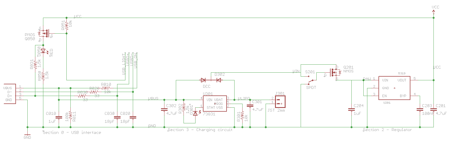
Let's take a closer look at the USB part:

For Google, this is the USB to LPC2148 SOFTCONNECT INTERFACE
Parts list:
| Quantity | Digikey Part | Value | Device | Part Numbers |
|---|---|---|---|---|
| 2 | 490-1281-1-ND | 18pF | CAP0402-CAP | C020, C030 |
| 1 | 490-3890-1-ND | 1μF | CAP0402-CAP | C010 |
| 1 | 350-2029-1-ND | RED | LED0603 | D050 |
| 1 | 455-2562-1-ND | USB_MICROB_JST | USB_MICROB_JST | J001 |
| 1 | BSS84-FDICT-ND | PMOS | MOSFET-PCHANNELSMD | Q050 |
| 2 | P10.0KLCT-ND | 10k | RESISTOR0402-RES | R010, R051 |
| 1 | P100KLCT-ND | 100k | RESISTOR0402-RES | R011 |
| 2 | P33.0LCT-ND | 33 | RESISTOR0402-RES | R020, R030 |
| 2 | P1.50KLCT-ND | 1.5k | RESISTOR0402-RES | R031, R050 |
A bit about the genealogy of this circuit. I originally got it from the Sparkfun Logomatic, which apparently was adapted from the Keil MCB2140 board, as explained by microbuilder.eu. All of these parts have a bunch of stuff not explained anywhere, and not mentioned on the LPC2148 datasheet, as seen below:

I have made some further adaptations to reduce the pin count and eliminate the vile BJT transistor in favor of a good and virtuous FET. Someday I will explain why FETs are better, but they are. Use FETs when you can, and BJTs when you have to.
So, in part number order:
- C010 is required by the USB spec. There must be between 1μF and 10μF between Vbus and Gnd as seen from upstream. If there is too little, the downstream device could be damaged by inductive flyback from the wire as it is disconnected. If there is too much, the inrush current to charge all that capacitance will be too high. The Sparkfun circuit had 0.1μF here, seemingly out of spec, but as it turns out, some of the capacitors downstream in the charger circuit are visible also. The Sparkfun circuit as a whole is within specs. This capacitor used to be higher until I noticed all the capacitance visible downstream.
- R010 and R011 seem to be there to provide pull-up and pull-down if the USB plug is unplugged or shorted. If the plug is unplugged, there is a total of 110kΩ of pull-down, so that the pin has a defined non-floating value if it is input. If Vbus and Gnd are shorted, there is still 10kΩ of pull-down, and more importantly, if the controller pin is output and high, there is 10kΩ of current limit.
- R020 and R030 are required by the USB spec. There must be between 28Ω and 44Ω of termination resistance. Accounting for the internals of the LPC2148, there must be a 33Ω resistor in series with each data line, as called out by the data sheet above.
- C020 and C030, form the other half of a low-pass noise filter, when combined with R020 and R030. In this case, frequencies higher than 250MHz are filtered out. This prevents the channel from being used as a high-speed (480MHz) channel, but the LPC2148 isn't capable of this anyway.
- R031 is required by the USB spec. When the downstream device (in this case the LPC2148) is ready to communicate, it ties in a pull-up resistor to one of D- (if low-speed) or D+ (if full-speed). Since the LPC2148 is a full-speed device (12MHz, up to 12Mb/s) it ties to D+.
- Q050 is the SoftConnect switch. It is a P-channel FET used as a high-side switch, which takes a bit of explanation. In a P-channel device, the source is connected to high voltage, and the drain to ground. If the gate voltage is sufficiently lower than the source, the FET conducts. In this circuit, the source is connected to Vcc (3.3V) and the gate is connected to the USB_SOFTCONNECT (or USB_LIGHT) pin on the LPC2148. When that pin is low, the transistor turns on, and provides a low-resistance path to Vcc, in effect tying one end of R031 to Vcc, which tells the upstream host that this device is ready to communicate. When the pin is high, the transistor turns off, and that end of R031 is left floating.
- D050 and R050 form an LED chain which lights whenever Q050 is on, or in other words, when SoftConnect is activated.
- R051 is a pull-up resistor, so that when the LPC2148 is off or its SoftConnect pin is input (as it is just after reset) the transistor is off, since its gate is not floating.
On to the charging circuit. I use an MCP73831, programmed to charge at 100mA, since I am planning for a battery as small as 100mAh. I have added a diode network D302 since there is no clear description in the data sheet for the 73831 explaining what the circuit will do if there is USB power present but no battery. With this diode network, if USB is present but the battery is not, the USB line will directly power the load. If the battery is present but the USB is not, the battery will power the load. If both are present, the USB wins, and the charger just has to concern itself with the battery, not the load.
Finally, the regulator circuit, and why this entry is subtitled "You can't use an N-channel MOSFET as a high-side switch."
The regulator itself is a MIC5319, capable in principle of delivering 500mA. Not that this is needed with the IMUinator, but to provide for future design expansion. It is hooked up exactly as specified in its own datasheet. The interesting part is the switch between the regulator and battery. That switch is only rated for 100mA. So, I said, let's stick a FET in there. We pick a nice high-current, low resistance FET available in a SOT-23 package. Use the switch to turn on the FET, and the FET to turn on the resistor. And here is where I made my mistake. I chose an N-channel FET, because I wanted direct logic on the switch (switch on -> FET on) and I installed it on the high side so that the circuit would be grounded (except for a floating Vin) when the FET was off.
But, "You can't use an N-channel MOSFET as a high-side switch".The FET is more accurately a voltage-controlled resistor. When the gate-to-source voltage is high enough, the resistance drops, and effectively the FET is just a wire, with about 200mΩ of resistance. But, the voltage is gate-to-source, and the very fact of dropping resistance raises the source-to-ground voltage. The gate-to-ground voltage remains the same, but the gate-to-source voltage drops as the source-to-ground voltage rises. The switch turns itself off.
It's not quite this bad, but in a way it is worse. The device will find some stable in-between state, dependent on the voltage supplied and probably the load on the regulator output. This in-between state will not be high enough to actually do anything, but high enough to draw some power, and dissipate it right in the FET. With the USB plugged in, the input was about 4.67V and I was getting about 3.07V out of a 3.3V regulator, showing that the FET had stabilized at less than 3.3V, when I was expecting near 4.67V. When the battery was used, the value was about 2.7V, not even enough to run the LPC2148.
So, the possible solutions are:
- Use a P-channel FET. This is what I would do if I had caught the design flaw early enough. The circuit would be identical, just the opposite switch position would now be on. Unfortunately, P-channel FETs and N-channel FETs both have the same pin assignments, so the source on the P-channel is the same pin as the source on the N-channel. However, the P-channel FET needs to have its source connected to high voltage, not low, so the board design would have to change. Since I already waited almost three weeks for the board, I can't do this.
- Remove the FET entirely. This way we just connect the gate terminal on the board to the source, and use the mechanical switch as the main switch. Perfect if I could just remove that FET already soldered on the board, or if I built a new one with no FET, but I don't have those parts.
- Short the FET. Don't remove it, just put a wire over the FET from gate to source. This will guarantee the gate-to-source voltage is zero, and therefore that the FET is off all the time. In the mean time, the voltage applied to the gate is shorted past the source to the load.
Update the second 24 Apr 2013:
Thursday, September 22, 2011
Eagle autorouter tips
It's pretty easy to comb the net for trash-talk and criticism of the CadSoft Eagle autorouter. Honestly it's not very good. It's less good than I am at routing, and I'm not that good.
But, if you lack patience like I do, the autorouter is the way to go. You can set it loose on a problem, go get a soda, read some blogs, come back, and have an acceptable if not beautiful board.
I have gathered a couple of useful hints which has helped the success of my autorouting attempts enormously:
But, if you lack patience like I do, the autorouter is the way to go. You can set it loose on a problem, go get a soda, read some blogs, come back, and have an acceptable if not beautiful board.
I have gathered a couple of useful hints which has helped the success of my autorouting attempts enormously:
- Do a good job placing components. Consider the hardware subroutine advice below.
- Set the routing grid to a very small number. If you are using inches, set it to 1 mil. I think the routing time goes up with the inverse square of the grid size, so half the grid size takes four times longer, but often the router can find solutions with a smaller grid that elude it with a larger grid.
- Consider the shape of your board, and the general "grain" of the signals on it. On long, skinny boards like the Stick IMUinator, it may not be best to prefer horizontal and vertical. Most of your signals will want to go horizontal, forcing most of them to one side of the board. Consider doing the preferred directions diagonally. I learned this by watching the FreeRouting.net autorouter work on my design.
- Delete (not just rip up) your ground plane polygons. The autorouter doesn't seem to handle polygons well at all, but if the polygon is not there and it treats ground just like any other signal, it can usually handle it well.
- Be prepared to do a manual cleanup after the autorouter is done. Put back the ground planes, and rip up all the lines, but not the vias, in the ground signal. Sometimes, you will find it necessary to leave a wire which connects parts of the ground plane. This especially happens if your ground planes use thermals. Also just fix any general ugliness on the board. For instance, the autorouter loves to bring a signal out the side of a QFP pad (like on the controller in the IMUinator) and bring it as close as possible to another pin before turning. Fix these manually.
- Check if the router has done anything monumentally stupid. For instance on the Stick IMUinator, the main crystal has four pads, two of which need to be grounded and two which are the crystal terminals. These are diagonally opposed, so that the orientation of the crystal doesn't matter. But, the autorouter connected the two ground terminals across the middle of the part, leaving no space for the actual crystal terminals. So, it routed one crystal terminal over the river, through the woods, past Grandmother's house, and ended up with a signal about 10x longer than the other one on both sides of the board, braided with other signals for maximum crosstalk problems. To fix this, I ripped it all up, manually routed just the crystal signals, then let the autorouter have at it.
Thursday, September 15, 2011
Plans and Priorities
- Get a rocketometer working.
- Put together the Precision clock.
- Do a test flight of the rocketometer, analyze the data, and produce a track.
- Design an engine room for Arisa.
- Design a bridge that can control either Arisa or Yukari.
- Program the bridge to handle Yukari. Minimum success for AVC2012 complete.
- Take the rocketometer to a roller coaster and use it as a rollercoasterometer
- Buy that sweet 5-servo collective pitch helicopter as a new Arisa.
- Program the bridge to handle Arisa.
- Put the rocketometer in a sounding rocket and take it into space.
Hardware is not Software 1
As many of my readers know, I am working on an IMU suitable to be put into rockets, robots, smuggled onto rollercoasters, etc.
I took a quick trip to the local hobby store (I love living in Longmont, 3 blocks from HobbyTown USA) to check out the rockets which were payload capable. I was looking for something a bit smaller and more manageable than the Big Daddy. What I found is that all the payloaders had a payload bay of 1.0" diameter or larger. If I made the IMU narrower than 1.0", I could fit most rockets.
So, Gentlemen, Behold! The Stick IMUinator!

This board is 0.9" x 2.0" and includes:
Now, why is this post titled "Hardware is not Software"? Well, I had what I thought was a briliant idea at the time. I couldn't get the Eagle autorouter to work well with such a tightly packed board. So, my briliant idea was to lay out the board in sections:
The next step is to lay out each section on the board, independently. Here is where hardware is different than software. My idea was to lay out each section, get it as small and compact as I could, then put all the sections together. Each section would have its interface with the outside through a small single set of signals. Each interface would be represented in the section by a surface-mount part with 6mil pads spaced 6mil apart. For instance, the USB section had one interface with four signals, USB presence, D+, D-, and SoftConnect. So, I put down an interface part with four pins and ran those signals to those pins. Vbus was connected to a different single-pin interface. Ground was left free-roaming.
Each section except for section 4 would be completely manually routed. All the parts are carefully laid out in their sections. I was able to get the power supply (sections 0, 2, and 3) on the back of the board and with a single layer of traces. This left the other side of the board available for something large in area but simple in layout. I wanted the sensors, particularly the compass, as far from the power supply as possible. The MicroSD slot turned out to be the perfect part.
Section 4, the controller, interfaced with everything else, so it was the most complicated. I hand-routed the crystal, USB, and SPI0 interface, but just plopped down some interface parts for the rest and let the autorouter have at it.
Now any programmers out there immediately recognize my attempt a hardware subroutines. The idea is to break a problem down into smaller, easier-to-solve parts. Each part interacts with the other parts through a well-defined, reusable interface.
Well, in hardware you can't quite do that. In a sense, that's what ICs are, but anyone who has laid out a board with multiple ICs has scratched their heads and said, "Why in the world did they order the pins that way?" You just can't optimize hardware and maintain the clean interface. For instance, when laying out the controller, I had to plan which direction to orient it. This was dependent on where the other sections were, so this hardware layout of the controller is dependent on this particular hardware.
Finally I put all the sections together and wired together their interfaces. This is where I discovered why in the world they put the pins in the order they did. Sometimes you can optimize the routing of a section by re-ordering the pins. Only rarely does this re-ordering match what was done to the matching interface on the other section. So, you have to plan in space for the interface, including the necessary vias and other-side board space to get signals across each other.
Ultimately I had a layout I was happy with. I then took a leap of faith. I ripped up all the routes and let the autorouter have a crack a the whole board at once. It wasn't actually that big of a risk, as I knew that there was a solution. Now the autorouter had no trouble, mostly because all the parts were well laid out. It ended up with a better design than I had before. So, this works, but not quite like I planned it.
Summary of steps:
I took a quick trip to the local hobby store (I love living in Longmont, 3 blocks from HobbyTown USA) to check out the rockets which were payload capable. I was looking for something a bit smaller and more manageable than the Big Daddy. What I found is that all the payloaders had a payload bay of 1.0" diameter or larger. If I made the IMU narrower than 1.0", I could fit most rockets.
So, Gentlemen, Behold! The Stick IMUinator!

This board is 0.9" x 2.0" and includes:
- ADXL345 3-axis accelerometer, digital readout over SPI/I2C
- L3G4200D 3-axis rotation rate sensor, digital readout over SPI
- BMP085 barometric pressure and temperature sensor, digital readout over I2C
- HMC5883 3-axis magnetic sensor, digital readout over I2C
- LPC2148 microcontroller
- MicroSD card slot
- USB micro-B (matches all the newest smartphone jacks)
- LiPo battery charger compatible with the connectors Sparkfun puts on their batteries.
Now, why is this post titled "Hardware is not Software"? Well, I had what I thought was a briliant idea at the time. I couldn't get the Eagle autorouter to work well with such a tightly packed board. So, my briliant idea was to lay out the board in sections:
- Section 0 is the USB interface
- 2 is the regulator
- 3 the LiPo charger
- 4 is the microcontroller
- 5 and 6 are the two SPI sensors
- 7 is the MicroSD slot
- 1 and 8 are the two I2C sensors
The next step is to lay out each section on the board, independently. Here is where hardware is different than software. My idea was to lay out each section, get it as small and compact as I could, then put all the sections together. Each section would have its interface with the outside through a small single set of signals. Each interface would be represented in the section by a surface-mount part with 6mil pads spaced 6mil apart. For instance, the USB section had one interface with four signals, USB presence, D+, D-, and SoftConnect. So, I put down an interface part with four pins and ran those signals to those pins. Vbus was connected to a different single-pin interface. Ground was left free-roaming.
Each section except for section 4 would be completely manually routed. All the parts are carefully laid out in their sections. I was able to get the power supply (sections 0, 2, and 3) on the back of the board and with a single layer of traces. This left the other side of the board available for something large in area but simple in layout. I wanted the sensors, particularly the compass, as far from the power supply as possible. The MicroSD slot turned out to be the perfect part.
Section 4, the controller, interfaced with everything else, so it was the most complicated. I hand-routed the crystal, USB, and SPI0 interface, but just plopped down some interface parts for the rest and let the autorouter have at it.
Now any programmers out there immediately recognize my attempt a hardware subroutines. The idea is to break a problem down into smaller, easier-to-solve parts. Each part interacts with the other parts through a well-defined, reusable interface.
Well, in hardware you can't quite do that. In a sense, that's what ICs are, but anyone who has laid out a board with multiple ICs has scratched their heads and said, "Why in the world did they order the pins that way?" You just can't optimize hardware and maintain the clean interface. For instance, when laying out the controller, I had to plan which direction to orient it. This was dependent on where the other sections were, so this hardware layout of the controller is dependent on this particular hardware.
Finally I put all the sections together and wired together their interfaces. This is where I discovered why in the world they put the pins in the order they did. Sometimes you can optimize the routing of a section by re-ordering the pins. Only rarely does this re-ordering match what was done to the matching interface on the other section. So, you have to plan in space for the interface, including the necessary vias and other-side board space to get signals across each other.
Ultimately I had a layout I was happy with. I then took a leap of faith. I ripped up all the routes and let the autorouter have a crack a the whole board at once. It wasn't actually that big of a risk, as I knew that there was a solution. Now the autorouter had no trouble, mostly because all the parts were well laid out. It ended up with a better design than I had before. So, this works, but not quite like I planned it.
Summary of steps:
- Break your circuit up into logical sections on the schematic.
- Add an interface part and define clean interfaces in the schematic.
- Lay out each section of the board by itself, but keep in mind its interaction with the rest of the circuit.
- Pull all the sections together and plug in the interfaces. You now have an acceptable baseline design.
- Rip up all of the signals and let the autorouter play, to see if it can come up with a better answer.
Saturday, May 14, 2011
Safer Motor Control

So, I just took out this double negative. Now, the diode is on when pin 1 is high, which turns on Q1 and runs the motor. When there is no signal from the optocoupler input, Q1 is off and the motor is off. This is safe.
BAT is the high-current battery for the motors, usually a 7.2V rechargable or something like that. The exact voltage isn't important as long as it is within the power capability of the other components. Most of the parts on the power-side of the circuit are rated for 100V or more. M1 is the motor terminal for the high current motor. Q1 is an IRF540, an n-channel MOSFET. This means that the part is on when the gate (left terminal) is more positive than the source (bottom terminal). Q1 claims to be able to handle 28A. D1 needs to be able to handle this at least momentarily when the motor switches off. A 1N4007 is just barely able to handle this, it has a peak current of 30A for about 8ms.
Wednesday, April 27, 2011
Further AVC post-mortem and future plans
"Steve is one of the brightest guys I've ever worked with - brilliant; but when we decided to do a microprocessor on our own, I made two great decisions - I gave them [Steve Furber and Sophie Wilson] two things which National, Intel and Motorola had never given their design teams: the first was no money; the second was no people. The only way they could do it was to keep it really simple." -- Hermann Hauser, from the Gnuarm web siteIn a one-man organization, we replace people with time. I got the no people (time) part right, but not the no money. Towards the end I was burning out (or so I thought) and replacing $50 parts at an alarming rate.
So, for next year, a budget of $100 plus the parts I already have. Since those parts include almost an entire robot, I should be fine. Once the car works, another $100 for the helicopter, but not before.
I am not sure about things like a Dremel mini-drill-press or other hardware like that with purposes beyond building robots, but gotten for building robots.
Subscribe to:
Posts (Atom)